| CPC G02B 6/43 (2013.01) [G02B 6/1226 (2013.01); G02B 6/4212 (2013.01); H01L 31/02327 (2013.01); H01L 31/101 (2013.01); H01L 31/108 (2013.01)] | 10 Claims |
|
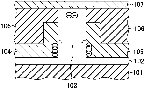
1. An optical device comprising:
a core on a substrate, wherein the core comprises a semiconductor material;
a first source electrode and a second source electrode respectively in contact with opposite side surfaces of the core that is interposed between the first source electrode and the second source electrode, wherein the first source electrode comprises a first metal material and the second source electrode comprises a second metal material, and wherein the core, the first source electrode, and the second source electrode together define a plasmonic waveguide; and
a drain electrode in contact with an upper surface of the core, wherein the drain electrode comprises a third metal material.
|