| CPC G02B 26/0858 (2013.01) [B06B 1/0207 (2013.01); G02B 26/10 (2013.01); G02B 27/0176 (2013.01); H03H 7/1708 (2013.01); H03H 7/175 (2013.01); G02B 2027/0154 (2013.01); H03H 2007/006 (2013.01)] | 20 Claims |
|
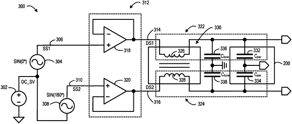
1. A display device, comprising:
a resonant scanning minor system comprising a scanning minor, a first mirror drive element, and a second minor drive element; and
a drive circuit configured to drive the scanning mirror at a resonant frequency, the drive circuit comprising
one or more signal sources configured to create a first source signal and a second source signal, the first source signal being 180 degrees out of phase with the second source signal;
a buffer stage configured to receive the first source signal and the second source signal and to output a first drive signal and a second drive signal;
a first resonant LC stage configured to amplify the first drive signal for provision to the first mirror drive element; and
a second resonant LC stage configured to amplify the second drive signal for provision to the second mirror drive element.
|