| CPC G02B 13/0045 (2013.01) [G02B 1/118 (2013.01); G02B 13/0085 (2013.01); H01L 27/14618 (2013.01); H01L 27/14621 (2013.01); H01L 27/14623 (2013.01); H01L 27/14627 (2013.01); H01L 27/14636 (2013.01); H01L 27/14645 (2013.01); H04N 23/55 (2023.01)] | 14 Claims |
|
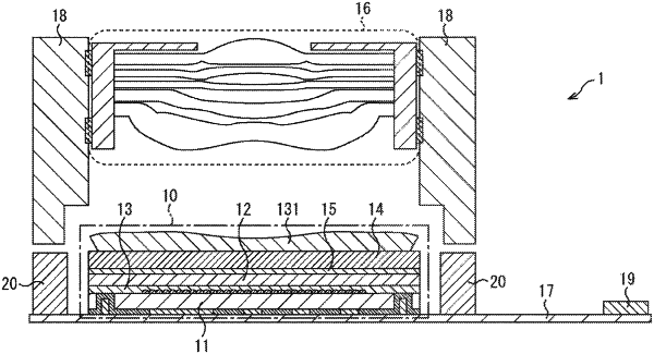
1. An imaging device, comprising:
a solid-state imaging element that generates a pixel signal by photoelectric conversion according to an amount of incident light;
a glass substrate;
a lens group that includes a plurality of lenses and focuses the incident light on a light receiving surface of the solid-state imaging element; and
a light shielding film,
wherein the glass substrate is disposed between the solid-state imaging element and the lens group,
wherein a lowermost layer lens included in the lens group and constituting a lowermost layer with respect to an incident direction of the incident light is provided on a first portion of a first surface of the glass substrate,
wherein the lowermost layer lens is an aspherical and recessed lens, and
wherein the light shielding film is formed on a side surface of the lowermost layer lens and on a second portion of the first surface of the glass substrate.
|