| CPC G01T 1/2018 (2013.01) [G01T 1/202 (2013.01)] | 17 Claims |
|
1. A micro image detector, comprising:
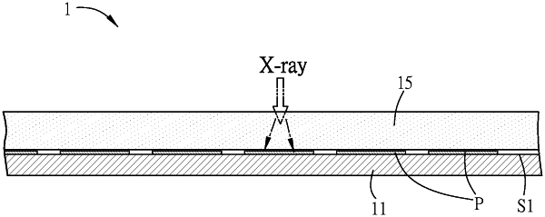
a substrate having a surface;
a circuit layer arranged on the surface of the substrate, wherein the circuit layer defines a plurality of detecting areas arranged in an array;
a plurality of light detecting elements disposed at the detecting areas and electrically connected with the circuit layer;
a plurality of driving elements disposed at the detecting areas and electrically connected with the circuit layer, wherein each of the driving elements drives one or more of the light detecting elements; and
a crystal scintillation layer arranged opposite to the substrate and covering the detecting areas;
wherein, the light detecting elements and the driving elements connect with the surface of the substrate, and at least one of the light detecting elements and the driving elements is formed by a process different from a process of forming the circuit layer on the substrate;
wherein the driving elements and the circuit layer are formed on the surface of the substrate by the same process; and
wherein the light detecting elements are transferred to the detecting areas by a mass transfer process.
|