US 11,940,536 B2
Light receiving element and ranging system
Tatsuki Nishino, Kanagawa (JP)
Assigned to SONY SEMICONDUCTOR SOLUTIONS CORPORATION, Kanagawa (JP)
Appl. No. 17/250,686
Filed by SONY SEMICONDUCTOR SOLUTIONS CORPORATION, Kanagawa (JP)
PCT Filed Aug. 16, 2019, PCT No. PCT/JP2019/032123
§ 371(c)(1), (2) Date Feb. 19, 2021,
PCT Pub. No. WO2020/045123, PCT Pub. Date Mar. 5, 2020.
Claims priority of application No. 2018-163584 (JP), filed on Aug. 31, 2018.
Prior Publication US 2021/0325538 A1, Oct. 21, 2021
Int. Cl. G01S 17/89 (2020.01); G01J 1/44 (2006.01); H04N 25/705 (2023.01)
CPC G01S 17/89 (2013.01) [G01J 1/44 (2013.01); H04N 25/705 (2023.01); G01J 2001/4466 (2013.01)] 9 Claims
OG exemplary drawing
 
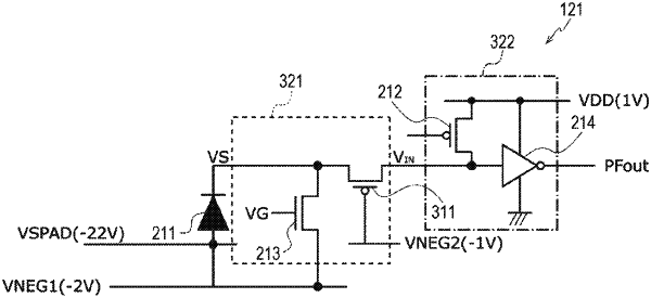
1. A light receiving element, comprising:
a pixel which includes:
an SPAD;
a first transistor configured to set a cathode voltage of the SPAD at a first negative voltage;
a voltage conversion circuit configured to convert the cathode voltage of the SPAD upon incidence of a photon and output the converted cathode voltage; and
an output unit configured to output a detection signal indicating the incidence of the photon on the SPAD, based on the converted cathode voltage.