| CPC G01S 15/8925 (2013.01) [G01S 7/539 (2013.01); G06V 10/98 (2022.01); G06V 40/1306 (2022.01); H01L 29/78666 (2013.01); H01L 29/78675 (2013.01); H01L 29/7869 (2013.01); H01L 29/78696 (2013.01)] | 28 Claims |
|
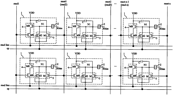
1. An ultrasonic fingerprint identification circuit, comprising a plurality of fingerprint identification units, each of the plurality of fingerprint identification units comprising:
an ultrasonic fingerprint identification sensor electrically connected to a first node, wherein the ultrasonic fingerprint identification sensor is configured to: convert a first electrical signal to an ultrasonic signal and radiate the ultrasonic signal towards a finger, and convert an ultrasonic signal reflected by the finger to a second electrical signal and transmit the second electrical signal to the first node;
a control circuit electrically connected to a composite signal line, the first node, and one first control signal line of a plurality of first control signal lines, wherein the control circuit is configured to: provide a reset potential to the first node in response to a first level provided by the one of the plurality of first control signal lines, and provide a pull-up potential to the first node in response to the first level provided by the composite signal line; and
a reading circuit electrically connected to the first node, a reading signal line, and one second control signal line of a plurality of second control signal lines, wherein the reading circuit is configured to read a detection signal of the first node in response to a first level provided by the one second control signal line,
wherein one of the plurality of first control signal lines electrically connected to one of the plurality of fingerprint identification units is reused as one of the plurality of second control signal lines electrically connected to another one of the plurality of fingerprint identification units;
wherein the control circuit comprises:
a switch unit electrically connected to the one first control signal line, and
a third transistor comprising a first terminal electrically connected to the first node, a second terminal electrically connected to the composite signal line, and a gate electrically connected to the second terminal of the third transistor through the switch unit;
wherein the switch unit comprises:
a fourth transistor comprising a gate electrically connected to the one first control signal line, a first terminal electrically connected to the gate of the third transistor, and a second terminal electrically connected to the second terminal of the third transistor, and
a diode comprising an anode electrically connected to the one first control signal line, and a cathode electrically connected to the gate of the third transistor; and
wherein a type of the fourth transistor is opposite to a type of the third transistor.
|