US 11,940,496 B2
Output voltage glitch reduction in ate systems
Michael E. Harrell, Colorado Springs, CO (US); Anthony Eric Turvey, Poughkeepsie, NY (US); Stefano I D'Aquino, Westford, MA (US); and Jennifer W. Pierdomenico, Temple, PA (US)
Assigned to Analog Devices, Inc., Wilmington, MA (US)
Appl. No. 17/904,931
Filed by Analog Devices, Inc., Wilmington, MA (US)
PCT Filed Feb. 24, 2021, PCT No. PCT/US2021/019368
§ 371(c)(1), (2) Date Aug. 24, 2022,
PCT Pub. No. WO2021/173635, PCT Pub. Date Sep. 2, 2021.
Claims priority of provisional application 63/114,775, filed on Nov. 17, 2020.
Claims priority of provisional application 62/980,772, filed on Feb. 24, 2020.
Prior Publication US 2023/0114208 A1, Apr. 13, 2023
Int. Cl. G01R 31/319 (2006.01); G01R 31/28 (2006.01); H03F 1/52 (2006.01); H03F 3/04 (2006.01); H03F 3/16 (2006.01)
CPC G01R 31/31924 (2013.01) [G01R 31/2834 (2013.01); H03F 1/523 (2013.01); H03F 3/04 (2013.01); H03F 3/16 (2013.01); H03F 2200/441 (2013.01)] 9 Claims
OG exemplary drawing
 
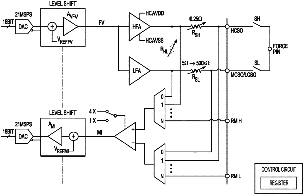
1. An automated testing system, the system comprising:
a high side switch circuit coupled to an input/output (I/O) connection;
a low side switch circuit coupled to the I/O connection;
a high side force amplifier (HFA) coupled to the high side switch circuit;
a low side force amplifier (LFA) coupled to the low side switch circuit;
an adjusting circuit coupled to the HFA and the LFA; and
a control circuit including a register, wherein the control circuit is configured to change the adjusting circuit by writing the register to change control of current at the I/O connection from one of the HFA or LFA to the other of the HFA or LFA.