| CPC G01R 31/311 (2013.01) [G01R 31/00 (2013.01); H01L 25/167 (2013.01); H01L 25/18 (2013.01); H01L 27/1443 (2013.01); H03K 17/687 (2013.01)] | 21 Claims |
|
1. A semiconductor device, comprising:
a semiconductor body;
an electrical device formed in an active region of the semiconductor body, the active region including an interface between the semiconductor body and an insulating material; and
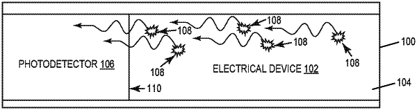
a sensor having a bandwidth tuned to at least part of an energy spectrum of light emitted by carrier recombination at the interface when the electrical device is driven between accumulation and inversion, wherein an intensity of the emitted light is proportional to a density of charge trapping states at the interface, wherein the sensor is configured to output a signal that is proportional to the intensity of the emitted light,
wherein the sensor is monolithically integrated in the same semiconductor body as the electrical device, and
wherein the sensor is formed in the active region of the semiconductor body.
|