| CPC G01R 31/2863 (2013.01) [G01R 31/2889 (2013.01)] | 16 Claims |
|
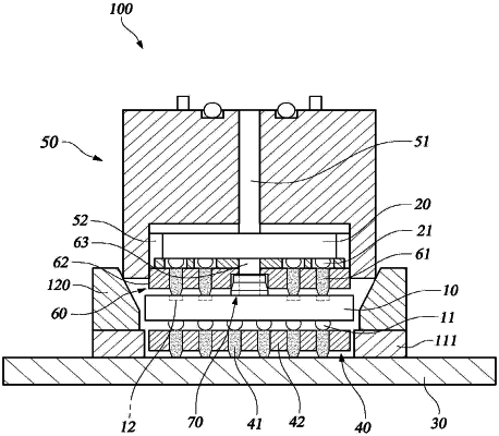
1. An apparatus for a semiconductor package, configured to test a package-on-package type semiconductor package, comprising:
an upper test socket on which an upper package is mounted, the upper test socket being mounted on a pusher and connected to a lower package placed therebelow;
a lower test socket mounted on a tester and connected to the lower package placed thereabove; and
an adsorption pad movably coupled to the pusher and configured to adsorb and pressurize the lower package using a vacuum pressure provided through the pusher,
wherein the adsorption pad comprising:
a body part having a vacuum pressure passage formed therein, and made of a silicon material; and
an adsorption part having a diameter greater than that of the body part, having an adsorption hole formed at a position corresponding to the vacuum pressure passage, and made of any one of a polyimide film, engineering plastic, and synthetic resin,
wherein the body part is attached on a central portion of an upper surface of the adsorption part and an outer oil overflow-preventing part configured to trap silicon oil eluted from the body part is formed at an outer periphery the adsorption part.
|