| CPC G01R 15/207 (2013.01) [H02K 11/27 (2016.01); H02K 2211/03 (2013.01)] | 28 Claims |
|
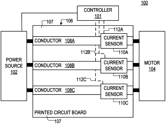
1. A substrate, comprising:
one or more first conductive layers;
one or more second conductive layers that are electrically coupled to the first conductive layers, the first conductive layers and the second conductive layers being arranged to form a conductor, the first conductive layers being arranged to define a first rift in the conductor; and
a dielectric material that is arranged to encapsulate, at least in part, the first conductive layers and the second conductive layers,
wherein the first rift is arranged to cause an area directly above the first rift to have a substantially uniform magnetic coupling coefficient.
|