| CPC G01R 1/06711 (2013.01) [G01R 1/07314 (2013.01)] | 20 Claims |
|
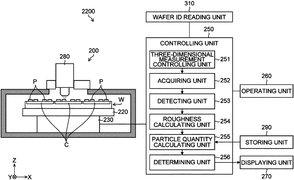
1. A particle measurement device configured to measure particles generated when a probe needle contacts an electrode pad of a wafer to check electrical characteristics of the wafer, the device comprising:
an acquiring unit configured to acquire pad surface shape data indicating a surface shape of the electrode pad including a probe needle mark where the probe needle has contacted;
a detecting unit configured to detect a pad reference surface as a reference for measurement of the particles from a surface of the electrode pad based on the pad surface shape data acquired by the acquiring unit;
a roughness calculating unit configured to calculate volume of a recessed portion recessed from the pad reference surface in the surface shape of the electrode pad and volume of a protruding portion protruding from the pad reference surface based on the pad surface shape data acquired by the acquiring unit; and
a particle quantity calculating unit configured to calculate a particle quantity from a volume difference between the volume of the recessed portion and the volume of the protruding portion which are calculated by the roughness calculating unit.
|