| CPC G01N 27/122 (2013.01) [G01K 7/20 (2013.01); H03K 17/60 (2013.01); H03K 17/6871 (2013.01)] | 16 Claims |
|
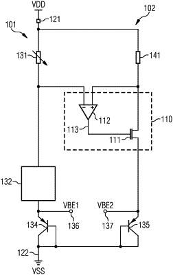
1. A circuit arrangement comprising:
a first branch comprising:
a terminal for a supply potential;
a resistor of variable resistance;
a bipolar transistor connected as a diode;
a terminal for ground potential connected to the bipolar transistor; and
a voltage shifter;
a second branch, comprising:
a resistor of fixed resistance, the resistor of fixed resistance connected to the resistor of the first branch;
another bipolar transistor connected as a diode, the terminal for ground potential connected to the other bipolar transistor; and
a transistor;
a control loop configured to reproduce a voltage drop at the resistor of variable resistance to a voltage drop at the resistor of fixed resistance;
an amplifier having input terminals connected to the resistors of the first and second branches and an output terminal configured to control the transistor of the second branch; and
an output terminal connected to the bipolar transistor of the first branch and another output terminal connected to the other bipolar transistor of the second branch, the output terminals configured to supply a differential voltage.
|