| CPC G01N 21/9501 (2013.01) [G01N 21/8806 (2013.01); G01N 21/95607 (2013.01); H01L 22/12 (2013.01); G01N 2021/95615 (2013.01); G01N 2021/95676 (2013.01)] | 9 Claims |
|
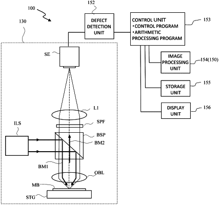
1. A defect inspection apparatus comprising:
a defect detection unit configured to acquire first defect information of a substrate; and
a comparative information acquisition unit configured to acquire a result of comparison between predetermined defect information stored in a storage unit and the first defect information, wherein
the substrate comprises multiple layers, and
wherein the substrate further comprises an optical thin film having a thickness of 10 nm or less as an outermost surface layer, and
wherein the comparative information acquisition unit is configured to acquire positional information on a defect where a part of the optical thin film is removed.
|