| CPC G01N 21/8851 (2013.01) [G06F 18/00 (2023.01); G06F 30/27 (2020.01); G06V 10/70 (2022.01); G06V 10/993 (2022.01); G06V 20/69 (2022.01); G01N 2021/8854 (2013.01)] | 20 Claims |
|
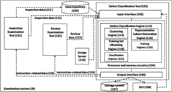
1. A computerized system of examining a semiconductor specimen, the system comprising a processing and memory circuitry (PMC) configured to:
obtain a plurality of defects of interest (DOIs) and a plurality of false alarms (FAs) from a review subset reviewed by a review tool, the review subset selected from a group of potential defects received from an inspection tool, wherein each potential defect is associated with a plurality of attribute values defining a location of the potential defect in an attribute space;
generate a representative subset of the group of potential defects, the representative subset comprising potential defects selected in accordance with a distribution of the group of potential defects within the attribute space, and indicate the potential defects in the representative subset as FAs; and
training a classifier using data informative of the attribute values of the plurality of DOIs, the potential defects of the representative subset, and respective indications thereof as DOIs or FAs, wherein the trained classifier is to be applied to at least some of the group of potential defects to obtain an estimation of a number of expected DOIs in the semiconductor specimen.
|