| CPC G01J 1/44 (2013.01) [G01J 1/0252 (2013.01); G01J 1/0411 (2013.01); G01J 1/0422 (2013.01); H01L 31/02327 (2013.01); H01L 31/024 (2013.01); H01L 33/58 (2013.01); H01L 33/644 (2013.01); G01J 2001/4466 (2013.01)] | 16 Claims |
|
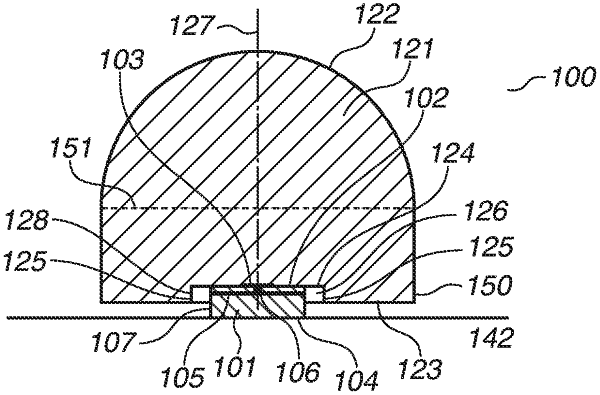
1. An electromagnetic wave module comprising a chip and a lens unit,
wherein the chip has a first face, a second face opposed to the first face, and a third face connecting the first face and the second face,
wherein the chip at least includes an antenna electrode disposed on the first face, a reference portion disposed on the second face and configured to determine a reference potential, and a semiconductor portion disposed between the antenna electrode and the reference portion and configured to perform gain action or rectification action on electromagnetic waves,
wherein the lens unit has a curved face forming a lens, a fourth face opposed to the curved face, and a recessed portion encompassed in an outer edge of the curved face on a projected plane in an optical axis of the lens,
wherein the recessed portion has a fifth face disposed at a position closer to the curved face than the fourth face, and a sixth face connecting the fifth face and the fourth face, and
wherein at least a part of the sixth face of the recessed portion is in contact with at least a part of the third face of the chip.
|