| CPC F21V 29/51 (2015.01) [F21V 9/40 (2018.02); F21V 19/0015 (2013.01); F21V 29/763 (2015.01)] | 7 Claims |
|
1. A light emitting device comprising:
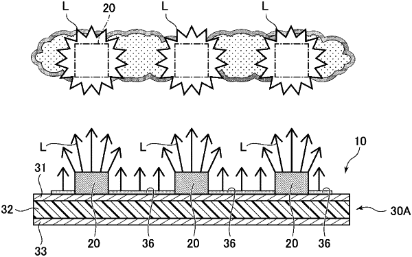
a light emitting substrate including an insulating substrate, a circuit pattern layer disposed on one surface of the insulating substrate, a plurality of light emitting elements bonded to the circuit pattern layer, and a phosphor layer that is disposed on the one surface of the insulating substrate without contacting a top surface of each of the plurality of light emitting elements and includes a phosphor in which a light emission peak wavelength, in a case where light emitted by at least one light emitting element of the plurality of light emitting elements is used as excitation light, is in a visible light region;
a flat heat pipe mechanism that removes heat from the light emitting substrate, a temperature of which is increased with light emission of the at least one light emitting element; and
a cooling unit that cools the flat heat pipe mechanism, wherein
the light emitting substrate emits a composite light of light emitting color of the at least one light emitting element and light emitting color of the phosphor layer, and
the flat heat pipe mechanism removes heat generated by the phosphor layer, a temperature of which is increased with light emission of the phosphor layer.
|