| CPC F21K 9/69 (2016.08) [F21V 23/003 (2013.01); G02B 27/30 (2013.01); F21S 8/085 (2013.01); F21S 41/151 (2018.01); F21Y 2103/10 (2016.08); F21Y 2115/10 (2016.08)] | 20 Claims |
|
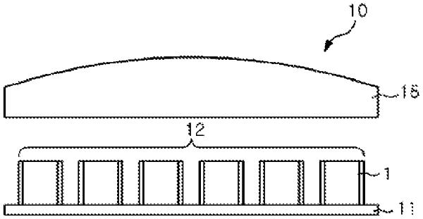
1. An illumination device, including:
a LED module; and
an optical system arranged in proximity to the LED module and configured to collimate light emitted by the LED module,
wherein the LED module includes:
a plurality of light sources for emitting excitation light;
a plurality of phosphors covering each of the plurality of light sources and configured to convert the excitation light into illumination light; and
a light blocking layer arranged on lateral surfaces of the plurality of phosphors;
wherein:
a first group of the light sources is arranged in a first linear array having first gaps between the light sources,
a second group of the light sources is arranged in a second linear array parallel to the first linear array and having second gaps between the light sources,
each of the plurality of phosphors has a light emitting surface having a size of 1 mm2 or less, and
at least one of the light sources in the first group is controlled separately from at least one of the light sources in the second group.
|