| CPC C30B 29/36 (2013.01) [C30B 23/02 (2013.01); C30B 33/10 (2013.01); H01L 21/30625 (2013.01); H01L 29/1608 (2013.01)] | 6 Claims |
|
1. A wafer manufacturing method, the method comprising:
arranging a raw material and a silicon carbide seed crystal to face each other in a reactor having an internal space;
controlling a temperature, a pressure, and an atmosphere of the internal space to sublimate the raw material, and grow a silicon carbide ingot from the silicon carbide seed crystal;
cooling the reactor, and recovering the silicon carbide ingot;
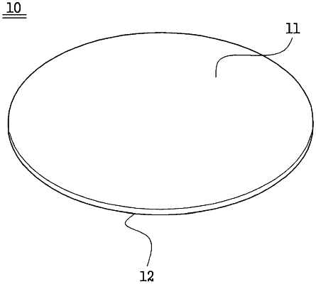
cutting the recovered silicon carbide ingot into a wafer; and
planarizing the wafer, and polishing a first surface of the planarized wafer,
wherein a heat insulating material surrounds an outer surface of the reactor, a heating device is configured to control the temperature of the internal space, and a density of the heat insulating material is 0.14 g/cc to 0.28 g/cc,
wherein the planarizing of the wafer comprises performing a first processing operation with a first grinding wheel which has a surface particle size of 1000 mesh to 3000 mesh, and performing a second processing operation with a second grinding wheel which has a surface particle size of 6000 mesh to 10000 mesh,
wherein the planarizing of the wafer further comprises performing a chemical mechanical polishing operation, and
wherein after chemical mechanical polishing is performed on the wafer, a total length of scratches on a first surface of the wafer is less than a diameter of the wafer, an averaae density of particles has a size of 0.3 μm or more is 3/cm2 or less, and an average density of micropipes on the first surface is 3/cm2 or less.
|