| CPC C23C 24/04 (2013.01) [H01J 37/321 (2013.01); H01J 37/32477 (2013.01); H01J 37/32715 (2013.01); C23C 16/4404 (2013.01); H01J 2237/2007 (2013.01); H01J 2237/3341 (2013.01); H01L 21/68757 (2013.01)] | 5 Claims |
|
1. A method of making a semiconductor manufacturing apparatus member having particle resistance, comprising steps of:
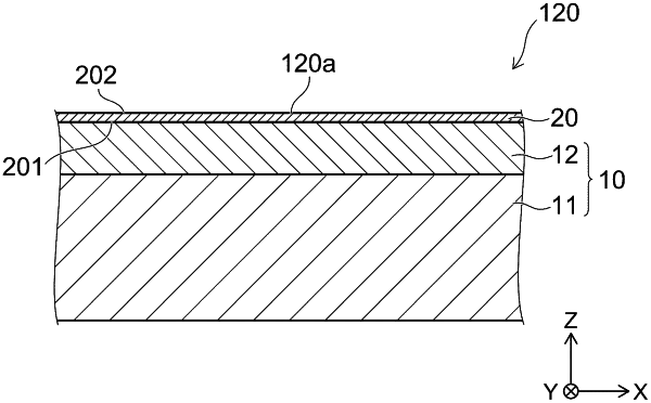
a) preparing a base comprising aluminum and having an alumite layer which is an anodic oxidation film at an upper surface of the base, wherein the alumite layer has a porous columnar structure, wherein a Young's modulus of the alumite layer is greater than 90 GPa and is less than or equal to 120 GPa; and
b) forming a particle-resistant layer of Y2O3 on the alumite layer by aerosol deposition, in which an aerosol containing fine particles of a brittle material dispersed in a gas is ejected from a nozzle to impact against a surface of the alumite layer, wherein the particle-resistant layer includes a polycrystalline ceramic;
wherein the particle-resistant layer has an arithmetic average height Sa of 0.060 μm or less after a reference plasma test is completed in which the semiconductor manufacturing apparatus member is exposed to a plasma.
|