| CPC C23C 22/57 (2013.01) [C09D 5/4411 (2013.01); C09D 5/4419 (2013.01); C23C 22/78 (2013.01); C25D 13/12 (2013.01)] | 15 Claims |
|
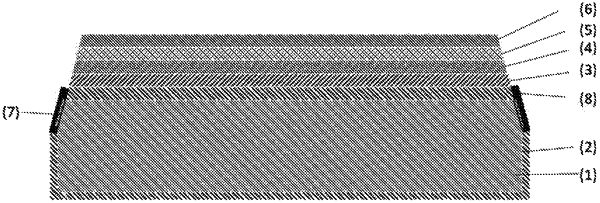
1. A coated metal alloy substrate for an electronic device, wherein the coated metal alloy substrate comprises a metal alloy substrate and at least one chamfered edge and further comprises:
a hydrophobic anti-fingerprint layer deposited on the metal alloy substrate;
a passivation layer deposited on the at least one chamfered edge; and
a water based paint layer deposited on the passivation layer, wherein portions of a lateral surface of the hydrophobic anti-fingerprint layer opposite from the metal alloy substrate are free of the passivation layer and the water based paint layer.
|