| CPC C23C 16/45536 (2013.01) [C23C 16/303 (2013.01); C23C 16/38 (2013.01); H01J 37/32009 (2013.01)] | 20 Claims |
|
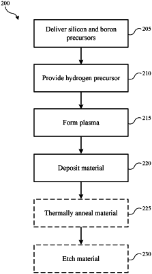
1. A method of depositing materials with reduced surface roughness, comprising:
delivering a silicon-containing precursor and a boron-containing precursor to a processing region of a semiconductor processing chamber;
providing a hydrogen-containing precursor with the silicon-containing precursor and the boron-containing precursor, wherein a flow rate ratio of the hydrogen-containing precursor to either of the silicon-containing precursor or the boron-containing precursor is greater than or about 1:1;
forming a plasma of all precursors within the processing region of a semiconductor processing chamber; and
depositing a silicon-and-boron material on a substrate disposed within the processing region of the semiconductor processing chamber.
|