| CPC C23C 16/45536 (2013.01) [C23C 16/45544 (2013.01); C23C 16/505 (2013.01); G01J 3/443 (2013.01); G01N 21/68 (2013.01); H01J 37/3244 (2013.01); H01J 37/32972 (2013.01); G01N 21/15 (2013.01); G01N 2201/08 (2013.01); H01J 2237/24485 (2013.01); H01J 2237/24507 (2013.01)] | 11 Claims |
|
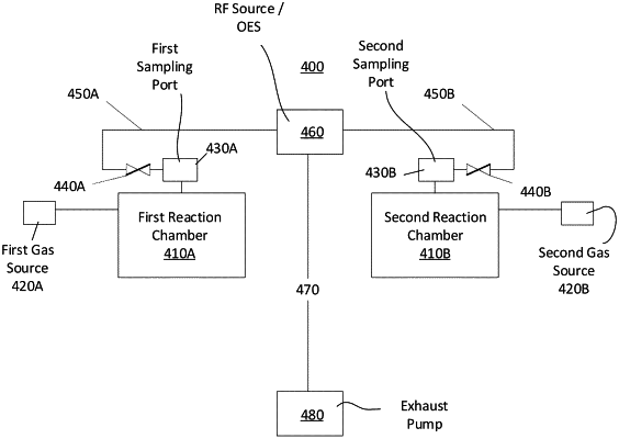
1. An apparatus configured for depositing a film on a semiconductor wafer comprising:
a first reaction chamber configured to hold a first semiconductor wafer;
a second reaction chamber configured to hold a second semiconductor wafer;
a first gas source configured to provide a first gas precursor to the first reaction chamber;
a second gas source configured to provide a second gas precursor to the second reaction chamber;
a first sampling port coupled to the first reaction chamber;
a second sampling port coupled to the second reaction chamber;
a RF source coupled to the first sampling port and the second sampling port, the RF source ionizing the first gas precursor and/or the second gas precursor;
an optical emissions spectrometer coupled to the RF source, the optical emissions spectrometer configured to obtain a light spectrum of the ionized first gas precursor and/or the ionized second gas precursor; and
an exhaust pump coupled to the RF source and configured to exhaust the ionized first gas precursor and/or the ionized second gas precursor;
wherein a concentration of the ionized first gas precursor and/or the ionized second gas precursor is determined based on the light spectrum.
|