| CPC C23C 16/45525 (2013.01) [C23C 16/01 (2013.01); C23C 16/12 (2013.01); C23C 16/45555 (2013.01); C23C 16/50 (2013.01); H01J 37/321 (2013.01); H01J 2237/334 (2013.01); H01L 21/3065 (2013.01)] | 21 Claims |
|
1. A method of fabricating a plate structure comprising:
creating a plate structure pattern in a silicon substrate, the plate structure pattern defining ridges that form a pattern;
depositing a layer of aluminum oxide (Al2O3) on a first side of the silicon substrate to form a patterned aluminum oxide;
removing the silicon substrate using reactive ion etching; and
using plasma-enhanced chemical vapor deposition to deposit a thin film on both sides of the patterned aluminum oxide,
wherein the plate structure has a thickness between about 1 nanometer (“nm”) and about 1 millimeter (“mm”).
|
|
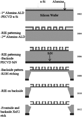
11. A method of fabricating a plate structure comprising:
depositing a first layer of aluminum oxide (Al2O3) on a first side of a substrate;
depositing a layer of sacrificial layer of amorphous silicon on top of the layer of the aluminum oxide;
etching the layer of amorphous silicon to form a hexagonal honeycomb pattern;
depositing a second layer of aluminum oxide (Al2O3) on the etched layer of amorphous silicon;
etching the second layer of aluminum oxide to at least create through holes to the layer of amorphous silicon;
removing the amorphous silicon and suspending the patterned first and second layers of aluminum oxide; and
using plasma-enhanced chemical vapor deposition to deposit a thin film on both sides of the patterned first and second layers of aluminum oxide.
|