| CPC C23C 14/5873 (2013.01) [C23C 14/14 (2013.01); C23C 14/588 (2013.01); C23C 16/01 (2013.01); F21V 7/26 (2018.02); F21V 9/32 (2018.02); H01S 5/0225 (2021.01); F21Y 2115/10 (2016.08); F21Y 2115/30 (2016.08)] | 17 Claims |
|
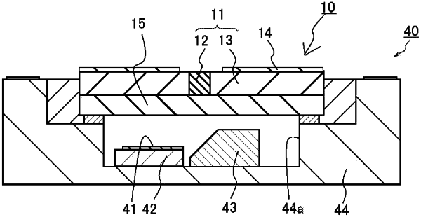
1. A method for manufacturing a wavelength conversion member, comprising:
providing a wavelength conversion layer having a phosphor-containing portion and a light reflecting portion surrounding the phosphor-containing portion, and the wavelength conversion layer having an upper surface, a bottom surface and at least one side surface;
forming a light-blocking film on the upper surface of the wavelength conversion layer; and
removing a part of the light-blocking film by laser processing to expose at least a part of the phosphor-containing portion from the light-blocking film.
|