US 11,939,647 B2
Tungsten target
Takafumi Dasai, Ibaraki (JP); and Shinichiro Senda, Ibaraki (JP)
Assigned to JX Metals Corporation, Tokyo (JP)
Appl. No. 16/494,375
Filed by JX Nippon Mining & Metals Corporation, Tokyo (JP)
PCT Filed Jan. 26, 2018, PCT No. PCT/JP2018/002559
§ 371(c)(1), (2) Date Sep. 16, 2019,
PCT Pub. No. WO2018/179770, PCT Pub. Date Oct. 4, 2018.
Claims priority of application No. 2017-070390 (JP), filed on Mar. 31, 2017.
Prior Publication US 2020/0016660 A1, Jan. 16, 2020
Int. Cl. C22C 27/04 (2006.01); B22F 3/10 (2006.01); B22F 3/14 (2006.01); B22F 3/15 (2006.01); C23C 14/34 (2006.01); B22F 1/05 (2022.01)
CPC C22C 27/04 (2013.01) [B22F 3/10 (2013.01); B22F 3/14 (2013.01); B22F 3/15 (2013.01); C23C 14/34 (2013.01); C23C 14/3414 (2013.01); B22F 1/05 (2022.01); B22F 2998/10 (2013.01)] 7 Claims
OG exemplary drawing
 
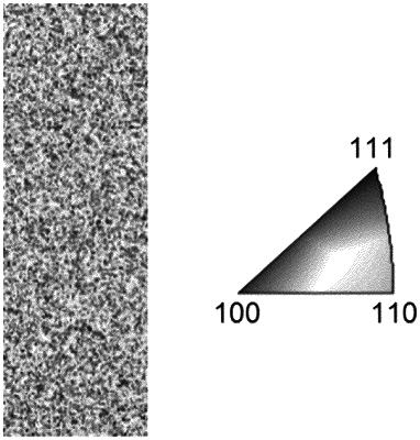
1. A tungsten sputtering target, wherein an area ratio of crystal grains having {100} planes oriented to a sputtering surface is in a range of 7.2 to 13.2%, an area ratio of crystal grains having {110} planes oriented to the sputtering surface is in a range of 20.4 to 23.4%, an area ratio of crystal grains having {111} planes oriented to the sputtering surface is in a range of 10.6 to 16.6%, and an area ratio in total of crystal grains having orientation planes oriented to the sputtering surface other than {100}, {11} and {111} planes is 46.8 to 62.1%, the area ratio being obtained by an analysis of a cross section perpendicular to the sputtering surface with an inverse pole figure mapping using electron backscatter diffraction.