| CPC B81C 1/00904 (2013.01) [B81C 1/00888 (2013.01); G02B 26/0833 (2013.01); G02B 26/105 (2013.01); B81B 2201/042 (2013.01); B81C 2201/0132 (2013.01); B81C 2201/0133 (2013.01); B81C 2201/0143 (2013.01)] | 14 Claims |
|
1. A method, comprising:
producing a semiconductor wafer, the semiconductor wafer comprising:
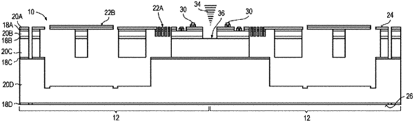
a plurality of microelectromechanical system (MEMS) semiconductor chips, wherein the plurality of MEMS semiconductor chips have MEMS structures arranged at a first main surface of the semiconductor wafer,
a first semiconductor material layer arranged at the first main surface, and
a second semiconductor material layer arranged under the first semiconductor material layer, wherein a doping of the first semiconductor material layer is greater than a doping of the second semiconductor material layer;
removing the first semiconductor material layer in a region between adjacent MEMS semiconductor chips; and
applying a stealth dicing process from the first main surface of the semiconductor wafer and between the adjacent MEMS semiconductor chips.
|