| CPC B81C 1/00015 (2013.01) [B81C 1/00476 (2013.01); B81C 1/00531 (2013.01); B81C 1/00539 (2013.01); B81C 2201/0105 (2013.01); B81C 2201/0198 (2013.01); B81C 2203/0172 (2013.01)] | 15 Claims |
|
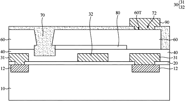
1. A manufacturing method of a MEMS device, comprising:
providing a substrate having at least one contact;
forming a first dielectric layer on the substrate, wherein the first dielectric layer has at least one through hole exposing a portion of a top surface of the contact;
forming at least one first metal layer on the first dielectric layer, wherein at least a portion of the first metal layer is electrically connected to the contact;
forming a second dielectric layer on the first dielectric layer and the first metal layer;
forming a sacrificial layer on the second dielectric layer;
forming a structure layer on the second dielectric layer and the sacrificial layer;
removing a portion of the structure layer to form a first opening, wherein the first opening exposes a portion of a top surface of the sacrificial layer;
removing a portion of the sacrificial layer through the first opening to form a second opening, wherein the second opening exposes a portion of a top surface of the second dielectric layer;
removing a portion of the second dielectric layer through the second opening to form a recess structure, wherein a cross-sectional area at a bottom of the first opening is smaller than a cross-sectional area at a top of the recess structure;
removing the sacrificial layer; and
forming a sealing layer, wherein at least a portion of the sealing layer is formed in the second opening and the recess structure, and the second dielectric layer, the structure layer, and the sealing layer define a chamber.
|