| CPC B32B 37/025 (2013.01) [H05K 1/0277 (2013.01); H05K 1/097 (2013.01); H05K 3/025 (2013.01)] | 11 Claims |
|
1. A method of fabrication of high resolution conductive patterns on polymeric substrates comprising:
a. forming a high resolution pattern with 3D features in a starting substrate;
b. forming an end product comprising a combination of a high-resolution conductive pattern based on the high resolution pattern on a polymeric substrate by:
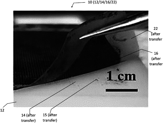
(1) creating a high resolution pattern on the starting substrate filled with a conductive material, coating the patterned conductive material on the starting substrate with a polymeric solution, drying the polymeric solution in a manner effective to promote adherence of the patterned conductive material to the dried polymeric layer, and peeling the dried polymeric layer and adhered conductive material from the starting substrate to transfer the dried conductive material in the high resolution pattern from the starting substrate to the dried polymeric layer.
|