| CPC B29C 45/02 (2013.01) [B29C 33/0061 (2013.01); B29C 33/0077 (2013.01); B29C 33/202 (2013.01); B29C 33/38 (2013.01); B29C 45/0046 (2013.01); B29C 45/03 (2013.01); B29C 45/14 (2013.01); B29C 45/14639 (2013.01); B29C 45/26 (2013.01); B29C 45/56 (2013.01); H01L 21/56 (2013.01); B29C 2033/023 (2013.01); B29C 2045/0051 (2013.01); B29C 2045/14852 (2013.01)] | 5 Claims |
|
1. A mold die, comprising:
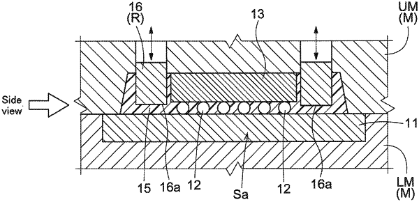
a mold die body that is configured to hold an object to be molded, the object including a substrate on which a plurality of protruding electrodes are arranged in a two-dimensional array and a chip mounted in a central area of the substrate and electrically connected to the protruding electrodes, and that has a cavity which is rectangular in a plan view and which is configured to receive a resin material, the cavity including lateral flow paths for the resin material to flow on lateral sides of the chip,
the mold die body including:
a pot for the resin material;
a gate disposed at one side of the cavity and configured to allow the resin material to flow into the cavity; and
a flow-path restricting mechanism that is disposed on both lateral sides of the cavity that are perpendicular to the one side and that is configured to narrow the lateral flow paths to reduce an amount of the resin material flowing through the lateral flow paths,
wherein the flow-path restricting mechanism includes a movable block disposed over the respective lateral flow path and configured to reduce the amount of the resin material flowing through the lateral flow path such that a leading end of each of the movable blocks coincides in a side view with a gap area between the substrate and the chip where the protruding electrodes are present, and
the movable block has a width of from 50% to 90% of a width of the lateral flow path.
|