| CPC A61N 1/0551 (2013.01) [A61B 5/4041 (2013.01); A61B 5/4893 (2013.01); A61B 5/6877 (2013.01); A61N 1/02 (2013.01); A61N 1/048 (2013.01); A61N 1/05 (2013.01); A61N 1/0529 (2013.01); A61N 1/0534 (2013.01); A61N 1/0539 (2013.01); A61N 1/36185 (2013.01); A61B 5/24 (2021.01); A61B 2018/00434 (2013.01); A61B 2562/125 (2013.01); A61N 1/0492 (2013.01)] | 20 Claims |
|
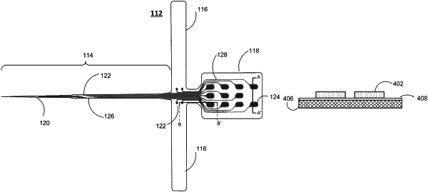
1. A method of manufacturing an implantable neural electrode comprising:
cutting a metal layer to form a plurality of electrode sites, contact pads and metal traces, wherein the metal layer is about 5 μm to 25 μm thick and wherein the metal traces connect one or more electrode sites to one or more contact pads;
forming a first silicone layer by:
knife-coating a polymer mesh with silicone, such that the first silicone layer has a thickness between about 50 μm and about 100 μm, and
curing the first silicone layer;
coupling the metal layer to the first silicone layer;
forming a second silicone layer by calendaring silicone to a thickness between about 50 μm and about 100 μm;
laminating the first silicone layer to the second silicone layer such that the metal layer is positioned between the first silicone layer and the second silicone layer;
forming a first set of holes in the first or second silicone layers to expose one or more electrode sites and a second set of holes in the first or second silicone layers to expose one or more contact pads in the metal layer;
after exposing the one or more contact pads, welding one or more wires to the one or more exposed contact pads; and
overmolding a third silicone layer over the one or more welded contact pads and a portion of the wires.
|