| CPC H10K 59/126 (2023.02) [H04M 1/0264 (2013.01); H04M 1/0266 (2013.01); H04N 23/57 (2023.01); H10K 50/844 (2023.02); G09G 2300/0426 (2013.01); G09G 2354/00 (2013.01); H04M 2250/52 (2013.01); H10K 59/122 (2023.02)] | 18 Claims |

|
1. An electronic device, comprising:
a display apparatus comprising:
a first substrate,
a driving circuit layer positioned on the first substrate, and the driving circuit layer comprising a plurality of thin film transistors in an array;
a pixel definition layer disposed on a side of the driving circuit layer away from the first substrate, the pixel definition layer comprising a plurality of pixel holes in an array, and each pixel hole receiving an organic light emitter and each of the organic light emitters correspondingly being connected to one thin film transistor;
a common electrode layer disposed on a side of the pixel definition layer away from the driving circuit layer;
a second substrate disposed on a side of the common electrode layer away from the pixel definition layer; and
a capping layer disposed between the second substrate and the common electrode layer;
a camera; and
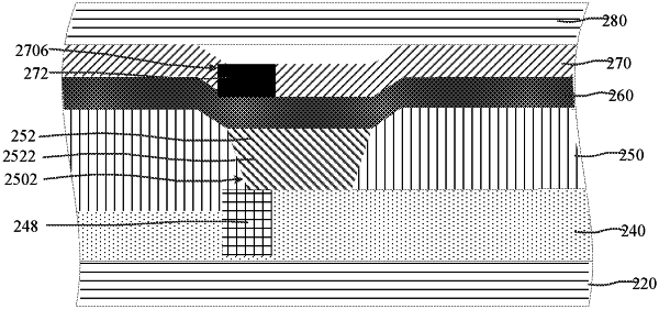
wherein at least a light shielding block is disposed between the second substrate and the organic light emitters, the light shielding block is at least partially corresponding to one of the thin film transistors the camera is at least partially positioned corresponding to the plurality of pixel holes and is configured to acquire images through the display apparatus and the light shielding block is configured to shield ambient light irradiating to the thin film transistors when the camera acquires an image;
wherein a face of the organic light emitter away from the light shielding block is in contact with a face of the thin film transistor away from the first substrate; and
wherein an orthogonal projection of the entire thin film transistor on the first substrate is within an orthogonal projection of the entire light shielding block on the first substrate.
|