| CPC H10B 43/27 (2023.02) [H10B 43/35 (2023.02)] | 13 Claims |

|
1. A method for forming a three-dimensional (3D) memory device, comprising:
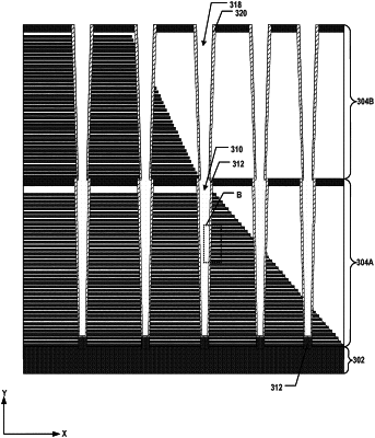
forming a first opening extending vertically through a first dielectric deck comprising a first plurality of interleaved sacrificial layers and dielectric layers above a substrate;
subsequently forming a high dielectric constant (high-k) dielectric layer and a channel sacrificial layer free of polysilicon along a sidewall of the first opening;
forming a second opening extending vertically through a second dielectric deck comprising a second plurality of interleaved sacrificial layers and dielectric layers on the first dielectric deck to expose the channel sacrificial layer in the first opening;
forming another high-k dielectric layer along the sidewall of the second opening;
removing the channel sacrificial layer in the first opening; and
subsequently forming a memory film and a semiconductor channel over the high-k dielectric layer along sidewalls of the first and second openings,
wherein after removing the channel sacrificial layer in the first opening, the high-k dielectric layer is in contact with the another high-k dielectric layer.
|