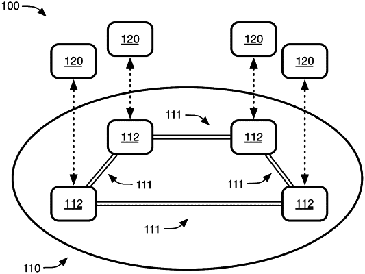
| CPC H04Q 11/0005 (2013.01) [H04B 10/25 (2013.01)] | 10 Claims |

|
1. An optical link system, comprising:
a photonics substrate;
a plurality of optical links, each optical link of the plurality of optical links comprising:
an optical waveguide defined on the photonics substrate;
a first optoelectronic transducer optically coupled to the optical waveguide; and
a second optoelectronic transducer optically coupled to the optical waveguide; and
a plurality of processing modules, each processing module of the plurality of processing modules comprising:
a respective electronics substrate mounted on the photonics substrate; and
a respective processor integrated circuit (IC) defined on the respective electronics substrate, each respective processor IC communicatively connected to other processing modules of the plurality of processing modules via respective optical links of the plurality of optical links, wherein each first optoelectronic transducer of the respective optical links is connected to the respective processor IC;
wherein the plurality of optical links communicatively couple each processing module of the plurality of processing modules directly to a plurality of other processing modules of the plurality of processing modules; and
wherein:
the plurality of processing modules define a rectangular array comprising a plurality of rows and a plurality of columns;
each row of the plurality of rows comprises a respective subset of at least three processing modules of the plurality of processing modules, wherein, for each row, each processing module of the row is communicatively connected directly to every other processing module of the row via a respective optical link of the plurality of optical links; and
each column of the plurality of columns comprises a respective subset of at least three processing modules of the plurality of processing modules, wherein, for each column, each processing module of the column is communicatively connected directly to every other processing module of the column via a respective optical link of the plurality of optical links.
|