| CPC H04N 25/75 (2023.01) [G05F 1/56 (2013.01); H04N 25/587 (2023.01); H04N 25/771 (2023.01); H04N 25/778 (2023.01)] | 16 Claims |
|
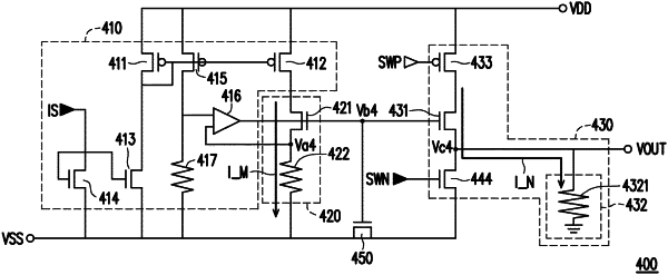
1. An output stage circuit, comprising:
a current source circuit;
a bias circuit coupled between the current source circuit and a ground terminal voltage; and
an output circuit, comprising:
a first transistor, wherein a control terminal of the first transistor is coupled to the bias circuit; and
a load circuit coupled to a second terminal of the first transistor and an output terminal;
a second transistor, wherein a first terminal of the second transistor is coupled to a supply voltage, and a second terminal of the second transistor is coupled to a first terminal of the first transistor; and
a third transistor, wherein a first terminal of the third transistor is coupled to the second terminal of the first transistor and the output terminal, and a second terminal of the third transistor is coupled to the ground terminal voltage,
wherein the bias circuit comprises:
a fourth transistor, wherein a first terminal of the fourth transistor is coupled to the current source circuit, a second terminal of the fourth transistor is coupled to the ground terminal voltage, and a control terminal of the fourth transistor is coupled to the control terminal of the first transistor and the first terminal of the fourth transistor, and
a reference resistor, wherein a first terminal of the reference resistor is coupled to the second terminal of the fourth transistor and the control terminal of the first transistor, and a second terminal of the reference resistor is coupled to the ground terminal voltage,
wherein the current source circuit comprises:
a fifth transistor, wherein a first terminal of the fifth transistor is coupled to the supply voltage;
a sixth transistor, wherein a first terminal of the sixth transistor is coupled to the supply voltage, a control terminal of the sixth transistor is coupled to a control terminal of the fifth transistor, and a second terminal of the sixth transistor is coupled to the bias circuit;
a seventh transistor, wherein a first terminal of the seventh transistor is coupled to a second terminal of the fifth transistor and the control terminal of the fifth transistor, and a second terminal of the seventh transistor is coupled to the ground terminal voltage; and
an eighth transistor, wherein a first terminal of the eighth transistor is coupled to a control terminal of the seventh transistor, a control terminal of the eighth transistor, and a current input terminal, and a second terminal of the eighth transistor is coupled to the ground terminal voltage.
|