| CPC H01L 31/03046 (2013.01) [H01L 31/036 (2013.01)] | 12 Claims |
|
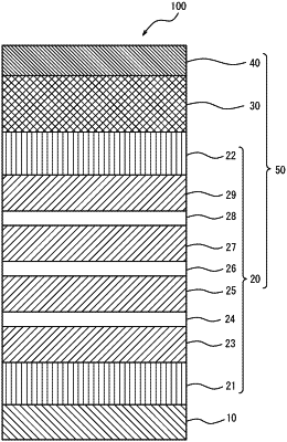
1. An infrared detecting device comprising:
a semiconductor substrate;
a first layer formed on the semiconductor substrate and having a first conductivity type;
a light receiving layer formed on the first layer; and
a second layer formed on the light receiving layer and having a second conductivity type, wherein
the first layer comprises, in the stated order: a layer made of InSb, a layer having a film thickness tx(1) in nanometers and containing Alx(1)In1-x(1)Sb; a layer having a film thickness ty(1) in nanometers and containing Aly(1)In1-y(1)Sb; and a layer having a film thickness tx(2) in nanometers and containing Alx(2)In1-x(2)Sb,
where ty(1), tx(1), tx(2), x(1), x(2), and y(1) satisfy the following relations:
0<ty(1)≤2360×(y(1)−x(1))−240(0.11≤y(1)−x(1)≤0.19),
0<ty(1)≤−1215×(y(1)−x(1))+427(0.19<y(1)−x(1)≤0.33),
0<ty(1)≤2360×(y(1)−x(2))−240(0.11≤y(1)−x(2)≤0.19),
0<ty(1)≤−1215×(y(1)−x(2))+427(0.19<y(1)−x(2)≤0.33),
0<x(1)<0.18, and
0<x(2)<0.18,
tx(1)≥200 nm,
tx(2)≥200 nm,
tx(1)>ty(1), and
ty(1)≤100 nm, and
the layer made of InSb is in contact with the semiconductor substrate and the layer containing Alx(1)In1-x(1)Sb;
wherein for an integer i from 1 to n (2≤n≤6), the first layer comprises: a layered structure in which a layer containing Alx(i)In1-x(i)Sb and a layer having a film thickness ty(i) in nanometers and containing Aly(i)In1-y(i)Sb are sequentially stacked on top of one another in the stated order in n layers; and a layer containing Alx(n+1)In1-x(n+1)Sb directly on the layer having a film thickness ty(n) in nanometers and containing Aly(n)In1-y(n)Sb,
where ty(i), x(i), x(i+1), and y(i) satisfy the following relations:
0<ty(i)≤2360×(y(i)−x(i))−240(0.11≤y(i)−x(i)≤0.19),
0<ty(i)≤−1215×(y(i)−x(i))+427(0.19<y(i)−x(i)≤0.33),
0<ty(i)≤2360×(y(i)−x(i+1))−240(0.11≤y(i)−x(i+1)≤0.19),
0<ty(i)≤−1215×(y(i)−x(i+1))+427(0.19<y(i)−x(i+1)≤0.33),
0<x(i)<0.18, and
0<x(i+1)<0.18;
wherein the layer containing Alx(i)In1-x(i)Sb has a film thickness tx(i) in in nanometers, and tx(i) and ty(i), satisfy the following relations:
tx(i)≥200 nm,
tx(i)>ty(i), and
ty(i)≤100 nm.
|