US 11,935,956 B2
TMD inverted nanowire integration
Kevin P. O'Brien, Portland, OR (US); Carl Naylor, Portland, OR (US); Chelsey Dorow, Portland, OR (US); Kirby Maxey, Hillsboro, OR (US); Tanay Gosavi, Portland, OR (US); Ashish Verma Penumatcha, Beaverton, OR (US); Shriram Shivaraman, Hillsboro, OR (US); Chia-Ching Lin, Portland, OR (US); Sudarat Lee, Hillsboro, OR (US); and Uygar E. Avci, Portland, OR (US)
Assigned to Intel Corporation, Santa Clara, CA (US)
Filed by Intel Corporation, Santa Clara, CA (US)
Filed on Jun. 26, 2020, as Appl. No. 16/913,835.
Prior Publication US 2021/0408288 A1, Dec. 30, 2021
Int. Cl. H01L 29/78 (2006.01); H01L 29/06 (2006.01); H01L 29/24 (2006.01); H01L 29/423 (2006.01); H01L 29/66 (2006.01); H01L 21/02 (2006.01)
CPC H01L 29/7853 (2013.01) [H01L 29/0673 (2013.01); H01L 29/24 (2013.01); H01L 29/42392 (2013.01); H01L 29/6653 (2013.01); H01L 29/6681 (2013.01); H01L 21/02568 (2013.01); H01L 21/0262 (2013.01)] 20 Claims
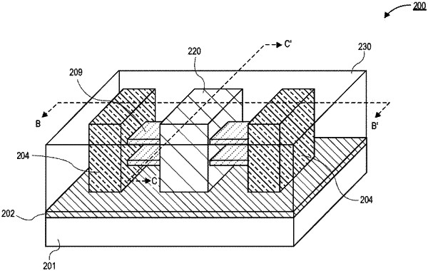
OG exemplary drawing
 
1. A semiconductor device, comprising:
a source contact;
a drain contact laterally spaced apart from the source contact; and
a two dimensional (2D) semiconductor channel laterally between the source contact and the drain contact, wherein the 2D semiconductor channel is a shell.