| CPC H01L 29/7455 (2013.01) [H01L 29/66363 (2013.01)] | 20 Claims |
|
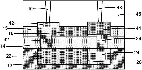
1. A structure for a silicon-controlled rectifier, the structure comprising:
a semiconductor substrate;
a first dielectric layer on the semiconductor substrate, the first dielectric layer having a thickness;
a first well in the semiconductor substrate beneath the first dielectric layer, the first well having a first conductivity type;
a second well in the semiconductor substrate beneath the first dielectric layer, the second well having a second conductivity type opposite to the first conductivity type, and the second well adjoining the first well along a first p-n junction;
a first terminal above the first dielectric layer;
a second terminal above the first dielectric layer;
a first connection having a first top surface above the first dielectric layer, the first connection extending from the first top surface through the thickness of the first dielectric layer between the first terminal and the first well; and
a second connection having a second top surface above the first dielectric layer, the second connection extending from the second top surface through the thickness of the first dielectric layer between the second terminal and the second well.
|