| CPC H01L 29/41775 (2013.01) [H01L 29/401 (2013.01); H01L 29/413 (2013.01)] | 14 Claims |
|
1. A semiconductor field-effect transistor (FET) device, comprising:
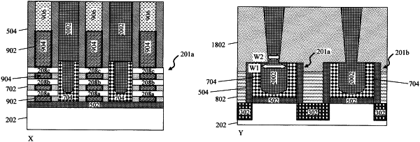
at least one gate; source and drains on opposite sides of the at least one gate; recesses in the source and drains; and metal contacts disposed over the source and drains and in the recesses, wherein the metal contacts are in direct contact with a bottom and sidewalls of each of the recesses in both a first direction and a second direction, wherein the first direction corresponds to a first vertical cut through the FET device that is perpendicular to the at least one gate and which crosses the metal contacts and the source and drains on the opposite sides of the at least one gate, and wherein the second direction corresponds to a second vertical cut through the FET device that is parallel to the at least one gate and is located through one of the source or drains, wherein the second direction is perpendicular to the first direction, wherein each metal contact includes a head section located within the recess of the source or drain and a shaft section extending above the source or drain, wherein the shaft includes a connecting section that connects the shaft to the head section, wherein the connecting section is wider than the head section in the first direction and the head section is wider than the connecting section in the second direction, the semiconductor FET device further comprising: a bottom dielectric isolation layer on which the source and drains are disposed; and dielectric spacers alongside the source and drains.
|