| CPC H01L 29/0821 (2013.01) [H01L 29/0649 (2013.01); H01L 29/0808 (2013.01); H01L 29/0817 (2013.01); H01L 29/1008 (2013.01); H01L 29/41708 (2013.01); H01L 29/735 (2013.01); H01L 29/737 (2013.01)] | 15 Claims |
|
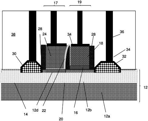
1. A structure comprising:
an extrinsic base region vertically over a semiconductor substrate and comprising asymmetrical sidewall spacers on opposing sidewalls of the extrinsic base region;
a collector region on the semiconductor substrate and separated from the extrinsic base region by at least a first spacer of the asymmetrical sidewall spacers;
an emitter region on the semiconductor substrate and separated from the extrinsic base region by a second spacer of the asymmetrical sidewall spacers;
a gate structure adjacent to the collector region; and
a sidewall spacer on the gate structure, wherein the sidewall spacer separates the gate structure from the collector region and the first spacer separates the gate structure from the extrinsic base region.
|