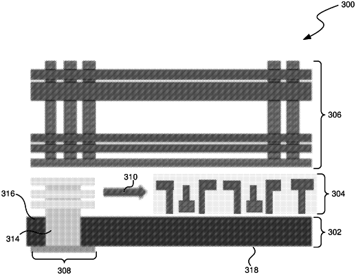
| CPC H01L 24/05 (2013.01) [H01L 21/4814 (2013.01); H01L 23/481 (2013.01); H01L 24/03 (2013.01); H01L 25/18 (2013.01); H10B 41/10 (2023.02); H10B 41/35 (2023.02); H10B 41/41 (2023.02); H10B 43/10 (2023.02); H10B 43/35 (2023.02); H10B 43/40 (2023.02); H01L 2224/05025 (2013.01); H01L 2924/13091 (2013.01); H01L 2924/1438 (2013.01)] | 20 Claims |

|
1. An apparatus, comprising:
a substrate of a memory die, the substrate comprising a frontside and a backside opposite the frontside;
control circuitry on the frontside of the substrate of the memory die;
a memory array on the memory die, the memory array over and electrically coupled to the control circuitry;
a through-silicon via (TSV) disposed under the memory array on the memory die, the TSV extending through the substrate of the memory die from the control circuitry to the backside of the substrate; and
a bond pad disposed on the backside of the substrate of the memory die and electrically coupled to the control circuitry via the TSV, wherein the bond pad, in connection with the TSV and the control circuitry, is configured to provide an interface between the memory array and one or more external components.
|