| CPC H01L 23/3672 (2013.01) [H01L 21/4882 (2013.01); H01L 23/552 (2013.01); H01L 23/66 (2013.01); H01L 2223/6677 (2013.01)] | 20 Claims |
|
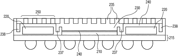
1. A semiconductor device package comprising:
a package substrate;
a semiconductor device die, comprising first and second opposing major surfaces, the first major surface mounted to the package substrate; and
a heat spreader element, comprising first and second opposing major surfaces, wherein
the heat spreader element is comprised of a thermally and electrically conductive material,
a first portion of the first major surface of the heat spreader element is thermally coupled to the second major surface of the semiconductor device die,
the heat spreader element comprises a plurality of structures formed on the second opposing major surface of the heat spreader element in a region opposing the portion of the first major surface coupled to the semiconductor device die, and
the heat spreader element further comprises one or more openings formed through the heat spreader element in a portion of the semiconductor device package having an antenna structure.
|