| CPC H01L 21/76897 (2013.01) [H01L 21/31144 (2013.01); H01L 21/76811 (2013.01); H01L 21/76883 (2013.01)] | 19 Claims |
|
1. A method of manufacturing a semiconductor structure, comprising:
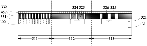
providing a base and a dielectric layer located on the base, wherein the base comprises an array region, a first circuit region and a second circuit region, and the first circuit region is located between the array region and the second circuit region; the base in the array region is provided with discrete capacitive contact plugs; the base in the first circuit region is provided with a first gate and the first circuit region is further provided with first conductive plugs on opposite sides of the first gate; the base in the second circuit region is provided with a second gate and the second circuit region is further provided with second conductive plugs on opposite sides of the second gate; the first gate, the second gate and the capacitive contact plugs are located within the dielectric layer; and a first conductive layer is formed on a top surface of the capacitive contact plugs;
forming a conversion layer and a target layer sequentially on the first conductive layer and the dielectric layer, wherein the target layer in the array region and the first circuit region is provided with first openings through the target layer, and a pattern density of the first openings in the array region is greater than a pattern density of the first openings in the first circuit region;
patterning the target layer between adjacent first openings in the array region to form a second opening through the target layer, and patterning the target layer in the first circuit region and the second circuit region to form a third opening through the target layer;
etching the conversion layer by use of the target layer having the first opening, the second opening and the third opening as a mask to form a first trench within the conversion layer;
forming a filling layer that fills the first trench and removing the conversion layer to form a second trench through the filling layer, wherein the second trench in the array region exposes a top surface of the first conductive layer, the second trench in the first circuit region exposes a top surface of the first conductive plug, and the second trench in the second circuit region exposes atop surface of the second conductive plug; and
forming a second conductive layer that fills the second trench.
|