US 11,935,755 B2
Method of producing a semiconductor laser and semiconductor laser
Alfred Lell, Maxhütte-Haidhof (DE); Georg Brüderl, Burglengenfeld (DE); John Brückner, Regensburg (DE); Sven Gerhard, Alteglofsheim (DE); Muhammad Ali, Regensburg (DE); and Thomas Adlhoch, Brennberg (DE)
Assigned to OSRAM OLED GmbH, Regensburg (DE)
Filed by OSRAM OLED GmbH, Regensburg (DE)
Filed on Dec. 18, 2020, as Appl. No. 17/126,907.
Application 17/126,907 is a division of application No. 16/335,968, granted, now 10,910,226, previously published as PCT/EP2017/077318, filed on Oct. 25, 2017.
Claims priority of application No. 10 2016 120 685.7 (DE), filed on Oct. 28, 2016.
Prior Publication US 2021/0111030 A1, Apr. 15, 2021
Int. Cl. H01L 21/285 (2006.01); H01L 21/268 (2006.01); H01L 33/00 (2010.01); H01S 5/042 (2006.01)
CPC H01L 21/28575 (2013.01) [H01L 21/268 (2013.01); H01L 33/005 (2013.01); H01S 5/04252 (2019.08); H01S 5/04254 (2019.08); H01L 21/28587 (2013.01); H01L 2933/0016 (2013.01); H01S 5/04256 (2019.08)] 18 Claims
OG exemplary drawing
 
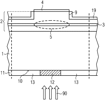
1. A semiconductor laser comprising:
a substrate having a semiconductor layer sequence with an active layer that generates light during operation of the semiconductor laser, and
a contact layer on a bottom side of the substrate opposite the semiconductor layer sequence,
wherein the contact layer has at least one first partial region and at least one second partial region which are formed contiguously,
the at least one first partial region is annealed, and
the at least one second partial region is unannealed.