| CPC H01L 21/02164 (2013.01) [H01L 21/02271 (2013.01); H01L 21/823462 (2013.01); H01L 29/51 (2013.01)] | 29 Claims |
|
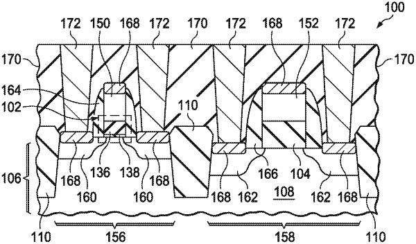
1. A semiconductor device, comprising:
a substrate including a semiconductor material;
a first dielectric layer on the semiconductor material, the first dielectric layer including an oxidized inhibitor layer and an oxidized semiconductor material layer located between the oxidized inhibitor layer and the substrate, the first dielectric layer having a first thickness; and
a second dielectric layer on the semiconductor material, the second dielectric layer having a second thickness,
wherein:
the second thickness is greater than the first thickness; and
the second dielectric layer extends further into the semiconductor material than the first dielectric layer.
|