US 11,934,080 B2
Mitigating defects in an electrochromic device under a bus bar
Sridhar K. Kailasam, Fremont, CA (US); Dhairya Shrivastava, Los Altos, CA (US); Zhiwei Cai, Fremont, CA (US); Robert T. Rozbicki, Saratoga, CA (US); Dane Gillaspie, Fremont, CA (US); Todd Martin, Mountain View, CA (US); Anshu A. Pradhan, Collierville, TN (US); and Ronald M. Parker, Olive Branch, MS (US)
Assigned to View, Inc., Milpitas, CA (US)
Filed by View, Inc., Milpitas, CA (US)
Filed on Dec. 15, 2020, as Appl. No. 17/247,541.
Application 17/247,541 is a division of application No. 16/249,822, filed on Jan. 16, 2019, granted, now 10,895,793.
Application 16/249,822 is a continuation of application No. 15/537,370, granted, now 10,520,783, issued on Dec. 31, 2019, previously published as PCT/US2015/065910, filed on Dec. 15, 2015.
Claims priority of provisional application 62/094,862, filed on Dec. 19, 2014.
Prior Publication US 2021/0103195 A1, Apr. 8, 2021
This patent is subject to a terminal disclaimer.
Int. Cl. G02F 1/153 (2006.01)
CPC G02F 1/153 (2013.01) [G02F 2201/501 (2013.01); G02F 2201/508 (2013.01)] 10 Claims
OG exemplary drawing
 
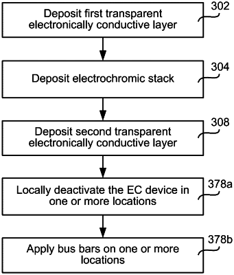
1. A method of manufacturing an electrochromic device comprising an electrochromic stack between a first and a second transparent electrically conductive layer configured to establish an electrical potential across the electrochromic stack and thereby cause optical switching of the electrochromic device, the method of manufacturing comprising:
(a) fabricating the electrochromic stack on a glass substrate without pre-patterning in a first facility;
(b) shipping the glass substrate including the electrochromic stack to a second facility; and
(c) performing post-processing in the second facility,
further comprising (d) deactivating the electrochromic stack under at least one of one or more bus bars applied on the glass substrate during post-processing.