| CPC G02F 1/025 (2013.01) [G02F 2203/50 (2013.01)] | 20 Claims |
|
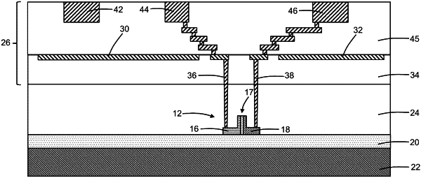
1. A structure comprising:
a semiconductor substrate;
a waveguide core on the semiconductor substrate, the waveguide core including a phase shifter; and
an interconnect structure over the waveguide core and the semiconductor substrate, the interconnect structure including a first plurality of interconnections, a first slotted shield, a first transmission line coupled to the phase shifter, and a second transmission line coupled to the phase shifter, the first transmission line laterally spaced from the second transmission line, the first slotted shield including a first plurality of segments, a first plurality of slots separating the first plurality of segments, a second plurality of segments, and a second plurality of slots separating the second plurality of segments, and the first plurality of segments of the first slotted shield positioned between the first transmission line and the semiconductor substrate,
wherein the first plurality of segments and the second plurality of segments are disposed on opposite side edges of the waveguide core, and a first minimum distance between the first plurality of segments and the second plurality of segments is less than a second minimum distance between the first transmission line and the second transmission line.
|