| CPC G02B 6/4269 (2013.01) [G02B 6/122 (2013.01); G02B 6/125 (2013.01); G02B 2006/12135 (2013.01); G02B 2006/12142 (2013.01)] | 18 Claims |
|
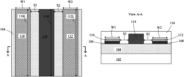
1. A semiconductor device comprising:
a first thermally conductive layer above a substrate;
a first semiconductor layer above a substrate, wherein the first thermally conductive layer is on the first semiconductor layer;
a second thermally conductive layer above the substrate, wherein the first thermally conductive layer and the second thermally conductive layer are electrically isolated;
a second semiconductor layer above the substrate, wherein the second thermally conductive layer is on the second semiconductor layer; and
an optoelectronic component above the substrate, the optoelectronic component is laterally between and spaced apart from the first semiconductor layer and the second semiconductor layer, the optoelectronic component is laterally between the first thermally conductive layer and the second thermally conductive layer, and the optoelectronic component is spaced apart from the first thermally conductive layer and the second thermally conductive layer.
|