| CPC G02B 6/1228 (2013.01) [G02B 6/0046 (2013.01); G02B 6/1225 (2013.01); G02B 6/14 (2013.01); G02B 2006/12035 (2013.01); G02B 2006/1215 (2013.01); G02B 2006/12152 (2013.01)] | 20 Claims |
|
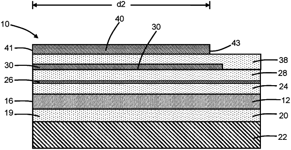
1. A structure for an edge coupler, the structure comprising:
a dielectric layer;
a waveguide core over the dielectric layer, the waveguide core including a tapered section; and
a back-end-of-line stack over the waveguide core and the dielectric layer, the back-end-of-line stack including a first interlayer dielectric layer, a second interlayer dielectric layer on the first interlayer dielectric layer, a side edge, a first feature, a second feature, a third feature laterally arranged between the first feature and the second feature, and a fourth feature, the first feature, the second feature, and the third feature positioned on the first interlayer dielectric layer adjacent to the side edge, the fourth feature positioned on the second interlayer dielectric layer over the third feature, the third feature terminating at a first end surface adjacent to the side edge and a second end surface opposite to the first end surface, the fourth feature terminating at a third end surface adjacent to the side edge and a fourth end surface opposite to the third end surface, the third feature overlapping with the tapered section of the waveguide core over a first distance between the first end surface and the second end surface, the fourth feature overlapping with the tapered section of the waveguide core over a second distance between the third end surface and the fourth end surface, and the second distance less than the first distance.
|