| CPC G01T 1/16 (2013.01) [G03F 7/0035 (2013.01); H10N 60/0128 (2023.02)] | 18 Claims |

|
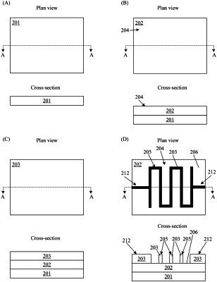
1. A process for hybrid subtractive-additive production of a superconducting multi-layer transition-edge sensor, the process comprising:
forming a superconductor layer on a substrate, the superconductor layer comprising a nascent topography;
forming a patterning photoresist on the superconductor layer such that the superconductor layer is interposed between the patterning photoresist and the substrate;
forming a sensor pattern in the patterning photoresist and exposing an exposed portion of the superconductor layer for removal;
subtractively forming, from the superconductor layer, the superconductor sensor layer comprising the sensor pattern by removing the exposed portion from the superconductor layer;
removing the patterning photoresist from the superconductor sensor layer;
forming a template photoresist on the superconductor sensor layer such that the superconductor sensor layer is interposed between the template photoresist and the substrate;
forming an inverse normal metal layer pattern in the template photoresist and exposing a bilayer portion of the superconductor sensor layer for addition of a normal metal layer; and
additively forming the normal metal layer comprising a normal metal pattern on the superconductor sensor layer such that the sensor pattern is interposed between the normal metal layer and the substrate to produce the superconducting multi-layer transition-edge sensor.
|