| CPC H10N 50/01 (2023.02) [H10N 50/10 (2023.02); H10N 50/80 (2023.02)] | 20 Claims |
|
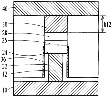
1. A method comprising:
forming a conductive via on a bottom electrode;
encapsulating the conductive via with a first dielectric layer;
forming a stack of magnetic tunneling junction (MTJ) layers on the conductive via;
forming a top electrode on the stack of MTJ layers; and
patterning the stack of MTJ layers and the first dielectric layer using the top electrode as a mask such that metal re-deposition material is formed on sidewalls of the patterned first dielectric layer, wherein the metal re-deposition material is prevented from interfacing with the conductive via by the patterned first dielectric layer being disposed on sidewalls of the conductive via.
|